The semiconductor repair industry is undergoing a profound transformation, driven by the rapid advancement of robotics and automation technologies. As demand for increasingly complex and miniaturized electronic components continues to grow, traditional repair methods are being challenged to keep pace. Robotics offers a solution, bringing unprecedented precision, efficiency, and reliability to semiconductor repair processes. This shift is not just enhancing repair capabilities; it’s revolutionizing the entire approach to maintaining and extending the life of critical semiconductor components.
Evolution of robotics in semiconductor repair
The journey of robotics in semiconductor repair has been marked by continuous innovation and adaptation. Initially, robots were primarily used for simple, repetitive tasks in semiconductor manufacturing. However, as technology advanced, so did the capabilities of these robotic systems. Today, they are integral to the repair process, handling tasks that were once thought to be the exclusive domain of highly skilled human technicians.
One of the most significant developments has been the introduction of micro-scale robotics. These systems can operate at the microscopic level, manipulating individual components with nanometer precision. This level of accuracy is essential when dealing with modern semiconductors, where the margin for error is measured in atoms rather than millimeters.
Another key evolution has been the integration of advanced sensors and machine vision systems. These allow robots to see and interpret their environment in real-time, making decisions based on complex visual data. This capability is crucial for identifying defects and guiding repair processes with unparalleled accuracy.
The integration of robotics into semiconductor repair processes represents a significant leap forward in the industry’s capabilities. From microscopic precision to AI-driven decision making, these technologies are reshaping how we approach the maintenance and longevity of critical electronic components. As semi-conductor robotic repair company continue to innovate, we can expect to see even more remarkable advancements in the field, pushing the boundaries of what’s possible in semiconductor technology.
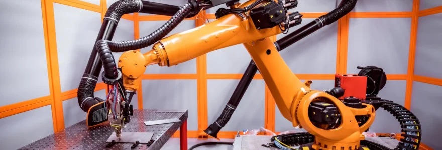
Advanced Robot-Assisted repair techniques
The advancement of robotics has given rise to a new generation of repair techniques that are pushing the boundaries of what’s possible in semiconductor maintenance. These techniques combine the precision of robotics with cutting-edge technologies to address even the most challenging repair scenarios.
Precision laser soldering with FANUC R-2000iC
The FANUC R-2000iC robot represents a significant leap forward in precision soldering technology. This robotic system utilizes advanced laser soldering techniques to perform repairs at the microscopic level. The robot’s arm can move with six degrees of freedom, allowing it to access hard-to-reach areas on complex semiconductor components.
The laser soldering process is controlled with incredible precision, with the robot able to adjust power, focus, and duration in real-time based on feedback from integrated sensors. This level of control ensures that repairs are completed without damaging surrounding components or introducing thermal stress to the semiconductor.
Automated optical inspection using cognex ViDi deep learning
Quality control is a critical aspect of semiconductor repair, and the Cognex ViDi deep learning system is revolutionizing this process. This AI-powered system uses advanced machine vision algorithms to inspect repaired semiconductors with a level of detail and consistency that surpasses human capabilities.
The ViDi system can detect defects as small as a few micrometers, identifying issues that might be invisible to the human eye. It can also learn from experience, improving its accuracy over time and adapting to new types of defects as they emerge. This continuous learning capability ensures that the inspection process remains effective even as semiconductor technologies evolve.
MEMS device repair with Nano-Manipulation robots
Micro-Electro-Mechanical Systems (MEMS) devices present unique challenges in repair due to their incredibly small size and delicate nature. Nano-manipulation robots have emerged as a solution to this challenge, offering the ability to interact with MEMS devices at the nanoscale.
These robots use piezoelectric actuators to achieve movements with sub-nanometer precision. They can perform tasks such as repositioning misaligned components, clearing nano-scale debris, and even manipulating individual atoms. This level of precision opens up new possibilities for repairing and optimizing MEMS devices that were previously considered irreparable.
Plasma cleaning and surface preparation robotics
Surface preparation is a critical step in many semiconductor repair processes, and plasma cleaning has emerged as a highly effective method. Robotic systems equipped with plasma cleaning capabilities can remove contaminants and prepare surfaces for repair with unprecedented precision and consistency.
These robots can adjust plasma parameters in real-time based on feedback from surface analysis tools, ensuring optimal cleaning results for each specific component. The automation of this process not only improves efficiency but also reduces the risk of contamination that can occur with manual handling.
AI integration in robotic semiconductor repair
The integration of Artificial Intelligence (AI) with robotic systems is taking semiconductor repair to new heights of efficiency and effectiveness. AI brings adaptive decision-making capabilities to robotic systems, allowing them to handle complex repair scenarios with a level of sophistication previously unattainable.
Machine learning for defect detection and classification
Machine learning algorithms are being employed to enhance the defect detection and classification process in semiconductor repair. These systems can analyze vast amounts of data from multiple sources, including optical inspections, electrical tests, and historical repair records, to identify patterns and predict potential failures.
By leveraging machine learning, repair robots can not only detect known defects but also identify emerging issues before they become critical. This predictive capability allows for proactive maintenance, reducing downtime and extending the lifespan of semiconductor components.
Predictive maintenance using IBM watson IoT platform
The IBM Watson IoT Platform is being utilized to implement predictive maintenance strategies in semiconductor repair facilities. This AI-powered system analyzes data from connected robotic repair systems, environmental sensors, and production schedules to predict when maintenance will be needed.
By anticipating maintenance needs, facilities can schedule repairs during planned downtime, minimizing disruptions to production. The system can also optimize maintenance schedules based on factors such as component criticality and repair complexity, ensuring that resources are allocated efficiently.
Real-time process optimization with NVIDIA jetson AI
NVIDIA’s Jetson AI platform is enabling real-time optimization of robotic repair processes. This edge computing solution allows for rapid processing of sensor data and decision-making at the point of repair, reducing latency and improving overall system responsiveness.
The Jetson AI can adjust repair parameters on the fly based on real-time feedback, ensuring optimal results even in variable conditions. This adaptive capability is particularly valuable in semiconductor repair, where small variations in temperature, humidity, or material properties can significantly impact repair outcomes.
Collaborative robotics in clean room environments
The introduction of collaborative robots, or cobots, into clean room environments is changing the dynamics of semiconductor repair. These robots are designed to work alongside human technicians, combining the precision and consistency of robotics with the adaptability and problem-solving skills of human operators.
Cobots in clean rooms are equipped with advanced sensors and safety features that allow them to operate in close proximity to humans without the need for protective barriers. This enables a more flexible and efficient repair process, where humans and robots can work together seamlessly on complex repair tasks.
One of the key advantages of collaborative robotics in semiconductor repair is the ability to quickly reconfigure repair processes. Cobots can be easily reprogrammed to handle different repair tasks, allowing facilities to adapt to changing repair needs without significant downtime or retooling.
Additionally, cobots are being used to enhance the capabilities of human technicians. For example, a cobot might assist a technician by holding components steady during delicate repair operations or by providing augmented reality overlays that guide the repair process. This symbiotic relationship between human and robot is pushing the boundaries of what’s possible in semiconductor repair.
Impact on semiconductor yield and quality control
The integration of robotics into semiconductor repair processes has had a profound impact on both yield and quality control. By minimizing human error and introducing unprecedented levels of precision and consistency, robotic repair systems are helping to improve the overall reliability and performance of semiconductor components.
Reduction in human error rates and contamination
One of the most significant benefits of robotic repair systems is the dramatic reduction in human error rates. Robots can perform repetitive tasks with unwavering accuracy, eliminating the variability that can occur with manual repairs. This consistency is particularly crucial in semiconductor repair, where even minor errors can have catastrophic consequences.
Moreover, robotic systems help to minimize contamination risks in clean room environments. Unlike human operators, robots don’t shed skin cells or hair, and they don’t require constant air exchanges to maintain breathability. This reduction in potential contaminants helps to improve overall yield rates and reduce the likelihood of defects caused by environmental factors.
Enhanced throughput with 24/7 robotic operations
Robotic repair systems can operate continuously, 24 hours a day, 7 days a week, without the need for breaks or shift changes. This continuous operation capability significantly enhances throughput, allowing repair facilities to process more components in less time.
The ability to operate around the clock also provides greater flexibility in scheduling repairs. Urgent repairs can be prioritized and completed quickly, while less time-sensitive tasks can be scheduled during off-peak hours to optimize resource utilization.
Improved traceability with robotic data logging
Robotic repair systems offer enhanced traceability through comprehensive data logging capabilities. Every action performed by the robot, along with environmental conditions and repair outcomes, can be recorded in detail. This wealth of data provides valuable insights for process improvement and quality control.
The detailed logs generated by robotic systems also facilitate compliance with industry regulations and quality standards. In the event of a quality issue, the repair history of a component can be easily traced and analyzed, allowing for rapid identification and resolution of problems.
Future trends: nanorobotics and Self-Healing semiconductors
As we look to the future of semiconductor repair, two emerging trends stand out: the development of nanorobotics and the advent of self-healing semiconductor materials. These innovations promise to further revolutionize the field of semiconductor maintenance and repair.
Nanorobotics represents the next frontier in precision repair. These microscopic robots, some as small as a few nanometers, could operate within semiconductor devices themselves, performing repairs at the atomic level. While still in the early stages of development, nanorobots could potentially extend the lifespan of semiconductors indefinitely by continuously monitoring and repairing damage at the molecular scale.
Self-healing semiconductors are another exciting development on the horizon. These materials would incorporate mechanisms to automatically repair minor damage without external intervention. For example, researchers are exploring the use of liquid metals that can flow into cracks or voids, restoring electrical connections. While this technology is still in its infancy, it has the potential to significantly reduce the need for external repairs and extend the operational life of semiconductor components.
As these technologies mature, they will likely be integrated with existing robotic repair systems, creating a multi-layered approach to semiconductor maintenance. This could lead to a future where semiconductor devices are not only repaired but continuously maintained and optimized throughout their lifecycle.